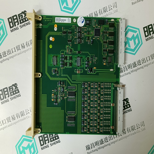
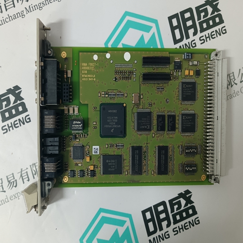
Home > Product > Robot control system > PACIFIC SCIENTIFIC SC904-001-01 Filter module
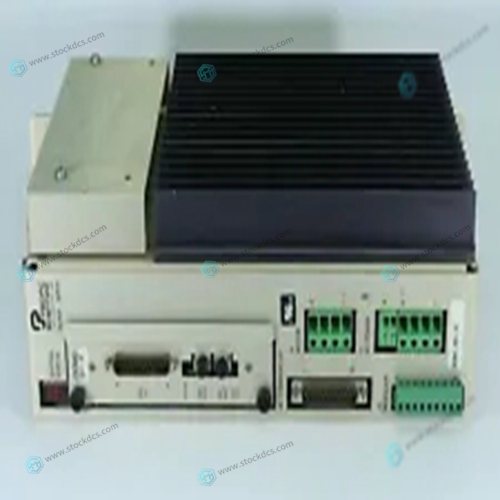
PACIFIC SCIENTIFIC SC904-001-01 Filter module
- Product ID: SC904-001-01
- Brand: OKUMA
- Place of origin: The United States
- Goods status: new/used
- Delivery date: stock
- The quality assurance period: 365 days
- Phone/WhatsApp/WeChat:+86 15270269218
- Email:stodcdcs@gmail.com
- Tags:PACIFIC SCIENTIFICSC904-001-01Filter module
- Get the latest price:Click to consult
PACIFIC SCIENTIFIC SC904-001-01 Filter module
DRAM Programming Considerations
❏ The DRAM map decoder can be programmed to accommodate different base address(es) and sizes of mezzanine boards.
❏ Onboard DRAM is disabled by a local bus reset and must be programmed before the DRAM can be accessed.
❏ Most DRAM devices require some number of access cycles before the DRAMs are fully operational. – Normally this requirement is met by the onboard refresh circuitry and normal DRAM installation. However, software should insure a minimum of 10 initialization cycles are performed to each bank of RAM.
Two mezzanine boards may be stacked to provide up to 256MB of onboard RAM (ECC). ❏ The MVME187 board and a single mezzanine board together take one slot. ❏ The stacked configuration requires two VMEboard slots.
Battery Backed Up RAM and Clock
The MK48T08 RAM and clock chip is a 28-pin package that provides
❏ A time-of-day clock
❏ An oscillator ❏ A crystal ❏ Power fail detection
❏ Memory write protection ❏ 8KB of RAM
❏ A battery The clock provides
❏ Seconds, minutes, hours, day, date, month, and year in BCD 24-hour format ❏ Automatic corrections for 28-, 29- (leap year), and 30-day months No interrupts are generated by the clock. The MK48T08 is an 8 bit device; however, the interface provided by the PCCchip2 supports 8-, 16-, and 32-bit accesses to the MK48T08. Refer to the MK48T08 data sheet for detailed programming information.
VMEbus Interface
The VMEchip2 provides:
❏ Local bus to VMEbus interface
❏ VMEbus to local bus interface
❏ Local-VMEbus DMA controller functions
❏ VMEbus system controller functions


Payment method and delivery
Shipment: EMS,DHL,UPS & FEDEX
Payment: T/T or Western Union
Professional seller
Professional sales of major electrical brand products in the world
Overseas direct purchase of products, authentic inventory, price concessions
After sales warranty, complete models, same products, different prices and services
