Home > Product > Robot control system > Nikon 4S017-319 Printed Circuit Board

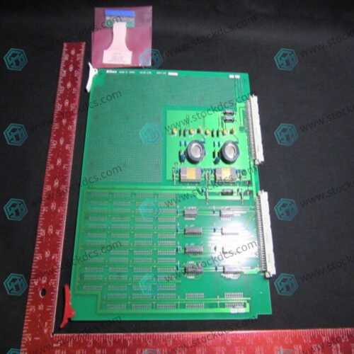
Nikon 4S017-319 Printed Circuit Board
- Goods status: new/used
- Delivery date: stock
- The quality assurance period: 365 days
- Phone/WhatsApp/WeChat:+86 15270269218
- Email:stodcdcs@gmail.com
- Tags:Nikon4S017-319Printed Circuit Board
- Get the latest price:Click to consult
Nikon 4S017-319 Printed Circuit Board
Product Details Introduction
Printed Circuit Board (PCB) is a basic component used to support and connect electronic components. It is usually a thin flat panel covered with conductive paths, connection points, and supporting structures for electronic components, used to build circuits. The following are some common features and functions of printed circuit boards:
Conductive path: There is a conductive path on a PCB, usually made of copper foil or other conductive materials, used to connect different electronic components and components, so that current can flow in the circuit.
Connection point: The connection point or pad on a PCB is usually used to connect electronic components, such as resistors, capacitors, integrated circuit chips, connectors, etc.
Component support: PCB provides a platform for installing and supporting electronic components to ensure they are in the correct position and can function properly.
Multi layer structure: Complex circuits typically require multiple layers of PCBs, where different layers are connected to each other through perforation or interconnection layers.
Printed markings: PCBs typically contain printed markings such as component locations, reference numbers, circuit diagram symbols, etc., for identification and maintenance by engineers and technicians.
Impedance matching: In high-frequency circuits, PCBs can be designed to meet specific impedance matching requirements to ensure the quality and stability of signal transmission.
Material: PCB usually uses glass fiber reinforced epoxy resin or other insulation materials as the substrate to ensure that electrical short circuits do not occur between electronic components.
Holes and SMD components: The PCB includes drilled holes for inserting or soldering SMD components through holes, such as surface mount devices (SMDs).
Interlayer connection: In multi-layer PCBs, conductive paths between different layers are connected through holes and interconnecting layers.
Printed Circuit: The circuit on a PCB is usually manufactured using printing technology, with conductive paths and connection points manufactured through printing or etching.
Heat dissipation: In some applications, PCBs are designed to aid in heat dissipation to ensure temperature control of electronic components.
Customized design: PCB can be customized according to specific circuit requirements, including hierarchy, connection point layout, materials, and dimensions.
Automated manufacturing: PCB is usually manufactured through automated production lines to ensure high quality and consistency.
Product image
Related products:
Nikon 4S017-615 Control Pulse Module