Home > Product > Robot control system > Nikon 4S020-067 Printed Circuit Board

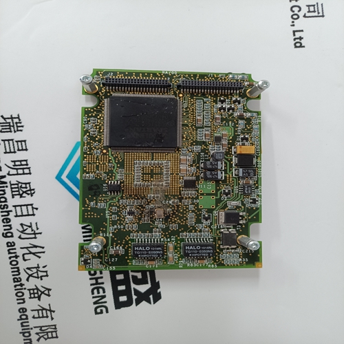
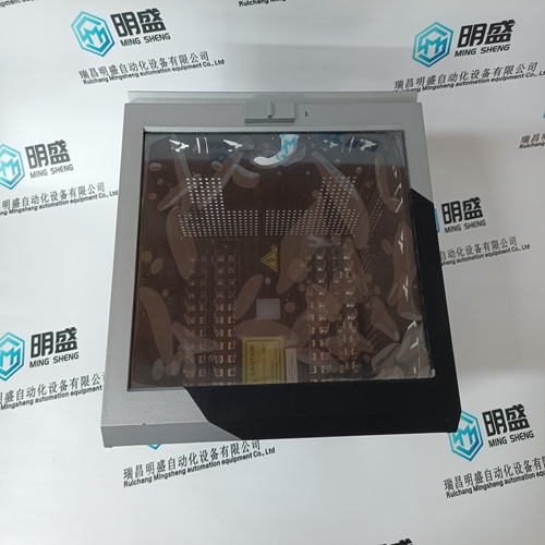
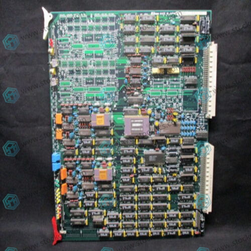
Nikon 4S020-067 Printed Circuit Board
- Goods status: new/used
- Delivery date: stock
- The quality assurance period: 365 days
- Phone/WhatsApp/WeChat:+86 15270269218
- Email:stodcdcs@gmail.com
- Tags:Nikon4S020-067Printed Circuit Board
- Get the latest price:Click to consult
Nikon 4S020-067 Printed Circuit Board
Product Details Introduction
The Nikon 4S020-067 Printed Circuit Board (PCB) has a variety of product features that can be customized according to specific application and design needs. The following are some common PCB product features:
Conductive path: The copper wires on the PCB form a circuit that allows current to flow through the connected electronic components, enabling signal transmission and data processing.
Multilayer structure: PCB usually has a multi-layer structure, including inner and outer layers. The inner layer is usually used for circuit connections, while the outer layer is usually used for component installation.
Printing technology: PCB manufacturing uses printing technology, where wires and connection points are formed on the substrate through chemical corrosion or etching.
Insulation material: PCB bodies are usually made of insulation materials, such as glass fiber reinforced epoxy resin (FR-4) or polyimide (PI).
Component installation: Electronic components on a PCB are installed through welding, plug-in, or surface mount (SMT) methods, connected to wires and connection points.
Signal integrity: The design of a PCB needs to consider signal integrity to ensure the quality of signal transmission, including reducing signal interference and latency.
Thermal management: For applications that require heat dissipation, PCBs may include heat dissipation solutions such as heat sinks, heat sinks, or heat dissipation vents.
Power management: PCBs typically include power management circuits to ensure that connected devices receive appropriate power.
Modular design: PCB usually adopts modular design, allowing for replacement or upgrading of different functional modules to meet different application requirements.
Surface coating: The wires and connection points on a PCB are usually coated to prevent corrosion and improve durability.
Solder resistance layer: The solder resistance layer on a PCB is used to cover some wires to protect the circuit from environmental influences.
Pad: A pad on a PCB used to connect electronic components, usually through welding or insertion.
Circuit tracking: Circuit tracking on a PCB is used to connect electronic components to the desired location, forming a circuit path.
Stray capacitance and inductance: When designing a PCB, it is necessary to consider stray capacitance and inductance to reduce circuit interference and fluctuations.
Mechanical compatibility: PCB design needs to consider compatibility with the casing and mechanical components to ensure proper installation and connection.
Product image
Related products:
Nikon 4S017-615 Control Pulse Module