Home > Product > Robot control system > Nikon 4S007-174-D PCB board

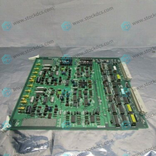
Nikon 4S007-174-D PCB board
- Goods status: new/used
- Delivery date: stock
- The quality assurance period: 365 days
- Phone/WhatsApp/WeChat:+86 15270269218
- Email:stodcdcs@gmail.com
- Tags:Nikon4S007-174-DPCB board
- Get the latest price:Click to consult
Nikon 4S007-174-D PCB board
Product Details Introduction
Printed Circuit Board (PCB) is a basic component used to support and connect electronic components. It is usually printed with a conductive copper layer on an insulating substrate. These circuits are used to transmit current, signals, and data to connect and organize electronic components, thus forming circuits.
Here are some key information about printed circuit boards (PCBs):
Main components:
Substrate: Usually made of insulating materials, such as glass fiber reinforced epoxy resin (FR-4) or polyimide (PI). The substrate provides physical support for the PCB and prevents short circuits between circuits.
Copper Layer: The copper layer is printed on the surface of the substrate, forming the wires and connection points in the circuit. They are made through chemical etching or other processing methods.
Circuit Traces: A circuit printed on a copper layer, used to connect electronic components, transmit signals, and current.
Pads and Holes: The connection point is usually located at the end of a circuit and is used to connect electronic components, such as soldering or inserting component pins. Holes are used to install connecting components or connect different layers of multi-layer PCBs through hole (PTH) technology.
Impedance Control Layer: For high-frequency circuits, a PCB may include an impedance control layer to ensure signal transmission quality.
Layers: A PCB can be a single layer (single sided), double layer (double sided), or multi-layer structure, with multiple copper layers inside, enabling more complex circuits.
Manufacturing process:
Manufacturing a PCB typically involves the following steps:
Design: Firstly, the circuit design engineer uses PCB design software to create the circuit diagram and layout of the PCB.
Printing: Based on design, the copper layer and other special layers of PCB are printed, usually using chemical etching methods.
Inspection and testing: The PCB is inspected and tested to verify its integrity and correctness.
Component installation: Electronic components (such as resistors, capacitors, integrated circuits, etc.) are installed on a PCB through welding or insertion.
Final testing: The functionality and performance of the entire PCB have undergone final testing to ensure its normal operation.
Application field:
PCB is widely used in various electronic devices and application fields, including but not limited to:
Consumer electronics: such as smartphones, tablets, televisions, sound systems, etc.
Computers and servers: including personal computers, workstations, and data center servers.
Communication equipment: such as routers, switches, base stations, and communication modules.
Medical equipment: including medical imaging equipment, patient monitoring equipment, and surgical tools.
Industrial automation: Used in automated production lines, robots, PLCs, and instruments.
Automotive electronics: including vehicle engine control, in car entertainment systems, driving assistance systems, etc.
Military and national defense: used for various military equipment and communication systems.
Product image
Related products:
Nikon 4S017-615 Control Pulse Module