Home > Product > Robot control system > Nikon 4S018-716AN Printed Circuit Board
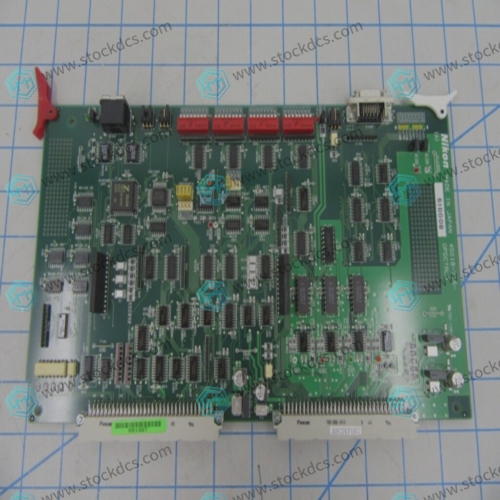
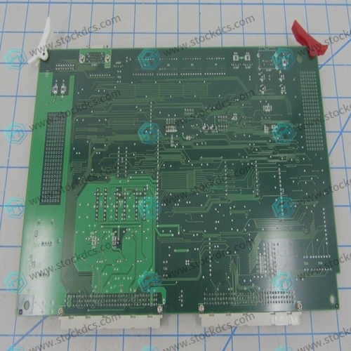
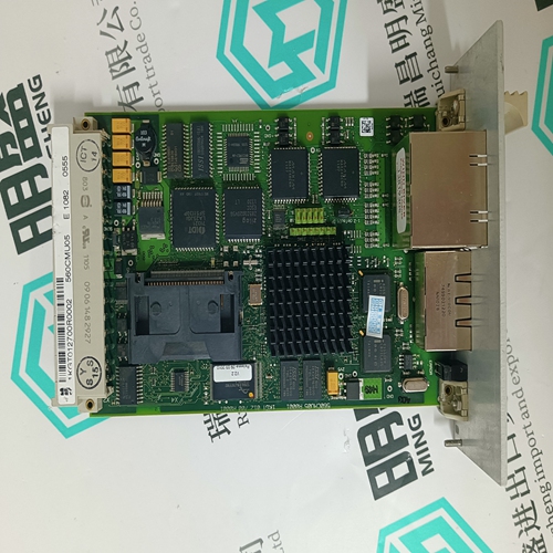
Nikon 4S018-716AN Printed Circuit Board
- Goods status: new/used
- Delivery date: stock
- The quality assurance period: 365 days
- Phone/WhatsApp/WeChat:+86 15270269218
- Email:stodcdcs@gmail.com
- Tags:Nikon4S018-716ANPrinted Circuit Board
- Get the latest price:Click to consult
Nikon 4S018-716AN Printed Circuit Board
Product Details Introduction
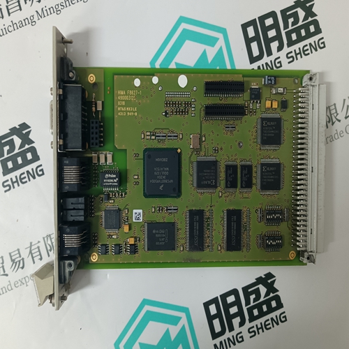
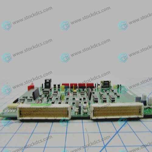
Nikon 4S018-716AN Printed Circuit Board (PCB) is a basic electronic component used to support and connect electronic components. A PCB typically includes one or more conductive paths on an insulating substrate, called circuits, used to transmit current and connect various electronic components. The following are some common product features of printed circuit boards:
Number of layers: A PCB can be a single-layer, double-layer, or multi-layer structure, depending on the complexity of the circuit and application requirements.
Materials: PCB can use different types of substrate materials, such as glass fiber reinforced resin (FR-4), aluminum substrate, ceramic substrate, etc., and can be selected according to needs.
Conductive path: The conductive path on a PCB is usually made of copper foil, which is printed on the substrate for connecting electronic components and transmitting current.
Holes and sockets: A PCB can include holes and sockets for connecting components, which are usually aligned with the pins of the component.
Pad: The area used for soldering component pins is usually called a pad, and they are usually coated to prevent corrosion.
Size and shape: PCBs can come in various sizes and shapes, and can be customized and designed according to the needs of specific applications and devices.
Component layout: The component layout and connection diagram on a PCB can be optimized based on the circuit design to maximize performance and maintainability.
Interlayer connection: Multilayer PCBs allow connections between different layers, which is crucial for complex circuit design and signal integrity.
Impedance control: In high-frequency applications, PCBs can be designed to control signal impedance to ensure signal quality.
Labels and identification: PCB usually includes labels and identification to distinguish different components and connections.
Welding technology: Different welding techniques can be used to connect components, including surface mount technology (SMT) and plug-in component welding.
Anti static measures: In some applications, PCBs may require anti static measures to protect electronic components from static damage.
Product image

Related products:
Nikon 4S019-259 Robot Interfac
其他网站链接