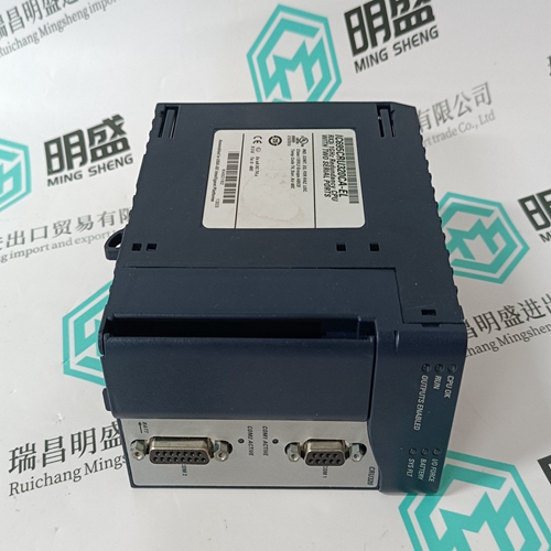
Home > Product > Robot control system > Nikon 4S018-382 Circuit Board
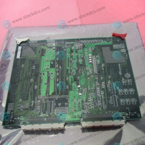
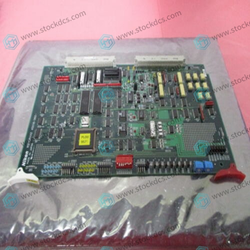
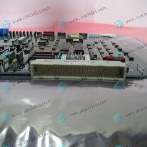
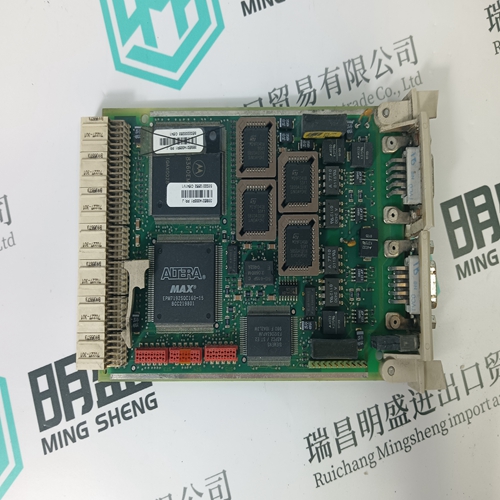
Nikon 4S018-382 Circuit Board
- Goods status: new/used
- Delivery date: stock
- The quality assurance period: 365 days
- Phone/WhatsApp/WeChat:+86 15270269218
- Email:stodcdcs@gmail.com
- Tags:Nikon4S018-382Circuit Board
- Get the latest price:Click to consult
Nikon 4S018-382 Circuit Board
Product Details Introduction
Nikon 4S018-382 Circuit Board, commonly referred to as PCB (Printed Circuit Board), is a basic electronic component used to support and connect electronic components. A PCB is a conductive path and connection point on an insulating material used to construct a circuit. The following are some common product features of circuit boards:
Number of layers: A PCB can be a single layer, double layer, or multi-layer structure, depending on the complexity of the circuit and application requirements.
Materials: PCB can use different types of substrate materials, such as glass fiber reinforced resin (FR-4), aluminum substrate, ceramic substrate, etc., and can be selected according to needs.
Conductive path: The conductive path on a PCB is usually made of copper foil, which is printed on the substrate for connecting electronic components and transmitting current.
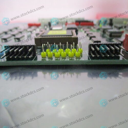
Holes and sockets: A PCB can include holes and sockets for connecting components, which are usually aligned with the pins of the component.
Pad: The area used for soldering component pins is usually called a pad, and they are usually coated to prevent corrosion.
Size and shape: PCBs can come in various sizes and shapes, and can be customized and designed according to the needs of specific applications.
Component layout: The component layout and connection diagram on a PCB can be optimized based on the circuit design to maximize performance and maintainability.
Interlayer connection: Multilayer PCBs allow connections between different layers, which is crucial for complex circuit design and signal integrity.
Impedance control: In high-frequency applications, PCBs can be designed to control signal impedance to ensure signal quality.
Labels and identification: PCB usually includes labels and identification to distinguish different components and connections.
Welding technology: Different welding techniques can be used to connect components, including surface mount technology (SMT) and plug-in component welding.
Anti static measures: In some applications, PCBs may require anti static measures to protect electronic components from static damage.
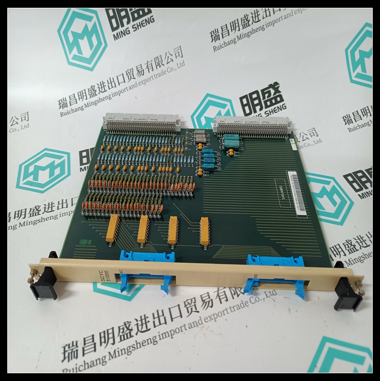
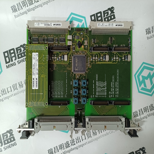
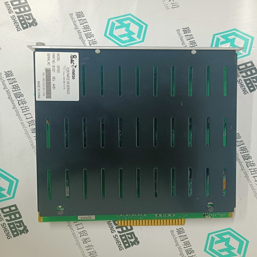
Product image

Related products:
Nikon 4S019-259 Robot Interfac
其他网站链接