Home > Product > Robot control system > Nikon 4S018-693 DUV Scanning System
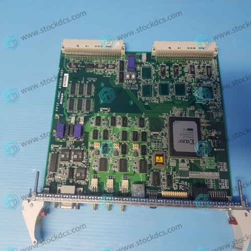
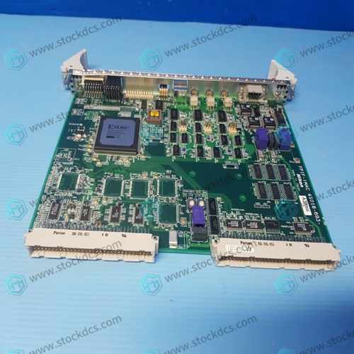
Nikon 4S018-693 DUV Scanning System
- Goods status: new/used
- Delivery date: stock
- The quality assurance period: 365 days
- Phone/WhatsApp/WeChat:+86 15270269218
- Email:stodcdcs@gmail.com
- Tags:Nikon4S018-693DUV Scanning System
- Get the latest price:Click to consult
Nikon 4S018-693 DUV Scanning System
Product Details Introduction
The Nikon 4S018-693 DUV scanning system is a deep ultraviolet (DUV) lithography technology system widely used in the semiconductor manufacturing industry, especially in integrated circuit (IC) manufacturing. This system uses deep ultraviolet light sources (typically with wavelengths between 193 nanometers and 248 nanometers) for pattern projection and lithography to manufacture tiny semiconductor devices and circuits. The following are some key features and application areas of the Nikon 4S018-693DUV scanning system:
Features:
Deep UV light source: The Nikon 4S018-693DUV scanning system uses a shorter wavelength deep UV light source, which can provide higher resolution and smaller feature size, thus supporting higher density integrated circuit manufacturing.
Projection lithography: The system includes a photomask and an optical lens for projecting patterns onto silicon wafers. These patterns include tiny circuit components, wires, transistors, and other microelectronic components.
High resolution: The Nikon 4S018-693DUV scanning system has high resolution and can achieve pattern resolution at the micron or submicron level, allowing for the manufacturing of smaller and more complex devices.
High precision: These systems typically have highly precise position control to ensure the accuracy of pattern alignment and overlap.
Multi layer exposure: Nikon 4S018-693DUV lithography typically uses multiple exposures to create complex device structures by stacking multiple patterns.
Photoresist: Photoresist is used in the lithography process to serve as a template and protection, allowing for the replication of desired patterns on silicon wafers.
Automation: Modern Nikon 4S018-693DUV scanning systems are typically equipped with automation features to improve production efficiency and reduce operator intervention.
Application field:
Semiconductor manufacturing: The Nikon 4S018-693DUV scanning system is widely used in semiconductor manufacturing to manufacture microprocessors, memory chips, sensors, and other semiconductor devices. They help manufacture smaller, faster, and more energy-efficient chips.
Microelectronics manufacturing: In addition to semiconductor manufacturing, Nikon 4S018-693DUV lithography technology is also applied to the manufacturing of MEMS (Micro Electro Mechanical Systems) and other microelectronic devices.
Integrated optical path manufacturing: In optical communication and optical device manufacturing, the Nikon 4S018-693DUV scanning system is used to manufacture high-performance optical devices and optical integrated circuits.
Lithography Template Manufacturing: Nikon 4S018-693DUV lithography technology is used to manufacture precision lithography templates for other lithography templates and printed circuit boards.
Product image

Related products:
Nikon 4S019-259 Robot Interfac
其他网站链接