Home > Product > Robot control system > ASML 4022.437.1312 Printed Circuit Board
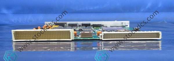
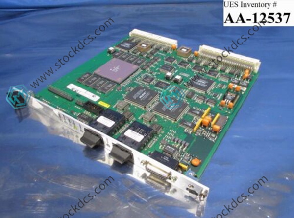
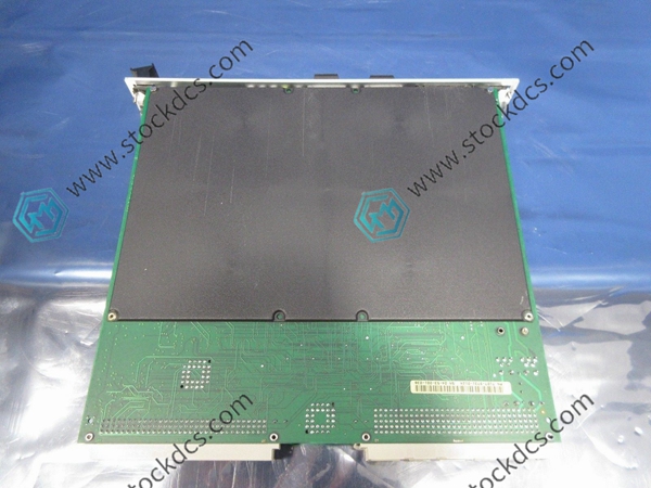
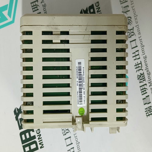
ASML 4022.437.1312 Printed Circuit Board
- Goods status: new/used
- Delivery date: stock
- The quality assurance period: 365 days
- Phone/WhatsApp/WeChat:+86 15270269218
- Email:stodcdcs@gmail.com
- Tags:4022.437.1312
- Get the latest price:Click to consult
ASML 4022.437.1312 Printed Circuit Board
Product Details Introduction
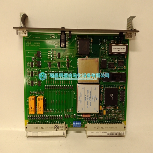
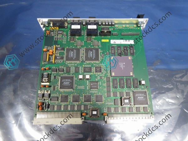
Printed Circuit Board (PCB) is a foundational department used to support and connect electronic components, typically used in the production of electronic equipment and circuits. A PCB is a thin and flat board that contains conductive gates and solder joints of electronic components, so that current can flow through the circuit and fulfill specific functions. Here are some key information about printed circuit boards:
Construction and organization: A PCB typically consists of one or more insulation layers, where conductive paths intersect. These conductive circuits are usually copper foil, which create junction points on the exterior or interior of the PCB. The different layers are connected through through-holes.
Conductive gate: A conductive gate or trace is a circuit between electronic components that communicates current and signals. These routes are usually accurately planned and manufactured to ensure the normal functioning of the circuit.
Electronic components: The electronic components on a printed circuit board include resistors, capacitors, transistors, integrated circuits, and other electronic components. They are usually connected to conductive circuits through welding or pulling out to exert influence in the circuit.
Printing technique: PCB is usually made through printing technique, where the patterns of conductive circuits and components are printed on insulation materials. This may be achieved through chemical decomposition, machine milling, inkjet printing, or other methods.
Single layer and multi-layer PCB: PCB may be single layer (single sided) or multi-layer (multi sided). Multilayer PCBs have multiple insulation and conductive layers for more complex circuit planning.
Application scope: PCB is widely used in various electronic equipment, including computers, mobile phones, televisions, communication equipment, conditioning equipment, automobiles, industrial control systems, aerospace equipment, and many other electronic products.
Customized planning: PCB is usually planned based on specific application needs, and the planning process includes decisions on circuit construction, trace planning, component arrangement, and connection form.
Non repairability: The planning and production of PCBs may affect the non repairability of equipment. A well planned PCB may make problem elimination and protection easier.
Green PCB: With the strengthening of environmental awareness, making environmentally friendly green PCBs has become more important. This includes data selection, waste disposal penalties, and acceptance.
Product image
Related products:
ASML 4022.634.20691 Fiber Opti
ASML 4022-639-92101 Laser Lamp
其他网站链接
