Home > Product > DCS control system > LAM 810-800082-243 Printed Circuit Board
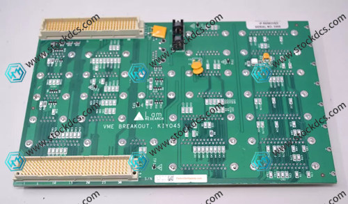
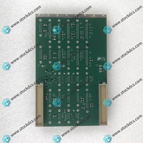
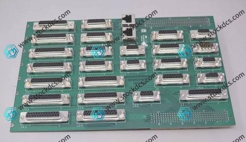
LAM 810-800082-243 Printed Circuit Board
- Goods status: new/used
- Delivery date: stock
- The quality assurance period: 365 days
- Phone/WhatsApp/WeChat:+86 15270269218
- Email:xiamen2018@foxmail.com
- Tags:
- Get the latest price:Click to consult
LAM 810-800082-243 Printed Circuit Board
Product Details Introduction
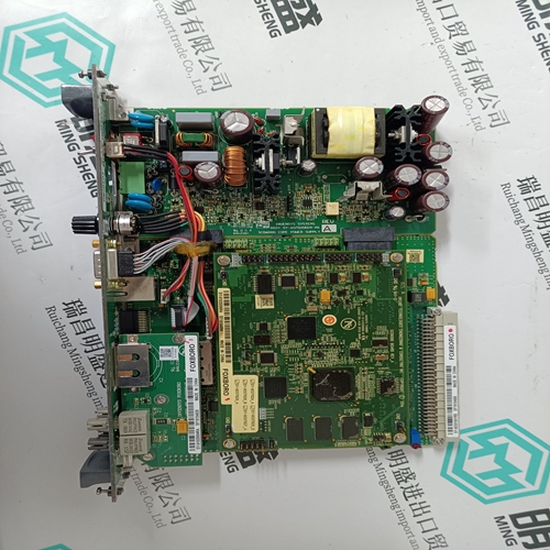
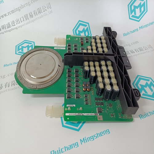
LAM 810-800082-243 printed circuit board (PCB) is a high-precision and high reliability circuit board produced by LAM Research, commonly used in semiconductor manufacturing equipment, especially in highly complex equipment such as chemical vapor deposition (CVD) and etching equipment. As one of the core components, it undertakes multiple functions such as signal transmission, power management, and device control.
Main features:
High quality materials
This PCB uses high-quality materials such as high-frequency substrates and precision metallization technology to ensure stable performance in complex and demanding environments.
Multi layer design
This printed circuit board typically has a multi-layer structure, ensuring sufficient signal transmission channels while reducing interference and optimizing electrical performance. Multi layer design improves its load-bearing capacity and signal transmission accuracy.
Durability and stability
Designed according to industrial standards, it has high resistance to heat, interference, and mechanical vibration. Especially suitable for long-term operation in high-temperature and high humidity environments of semiconductor manufacturing equipment.
Accurate signal processing
This circuit board is responsible for precise processing of various signals and can seamlessly communicate with other control systems through specific interface modules.
High density packaging technology
By adopting high-density packaging (such as SMT) and compact layout, the space utilization of the circuit board has been optimized, while improving electrical performance and response speed.
Typical applications:
Semiconductor manufacturing equipment
An automated control system for processes such as etching, thin film deposition, and ion implantation.
Chemical Vapor Deposition (CVD) Equipment
Used for precise control of gas flow rate, current, pressure, and other parameters in CVD reaction chambers.
Plasma cleaning equipment
Used for high-precision cleaning of semiconductor wafer surfaces to ensure high consistency of the process.
Automated testing equipment
Used for testing and analyzing the performance of semiconductor chips, supporting data transmission, processing, and analysis.
Technical parameters (assuming reference, specific model and application need to be confirmed):
Size: Customized sizes are usually provided based on the design and installation requirements of the equipment.
Power requirements: According to electrical design, common operating voltages are+12V DC and+24V DC, depending on equipment requirements.
Working temperature range: Suitable for industrial environments, typically ranging from -20 ° C to+70 ° C.
Connection interface: usually supports various industrial standard interfaces, such as USB, Ethernet, RS-232, etc.
Signal types: including analog signals, digital signals, and high-frequency signal processing.
PCB Layers: Generally designed in multiple layers to accommodate complex circuits and compact layout requirements.
Product imag
Related website links
HONEYWELL 05704-A-0146 Digital
PROSOFT MVI46-MCM communicatio
ABB 3DDE300417 Input/Output Board
Other website links
| 6ES5497-4UD11 | 6SC9111-2AF2 | TRICONEX 3807 |
| 6ES5490-8MB11 | CACR-SR07BB1AM-Y15 | 6ES5242-1AA13 |
| 6ES5490-7SA21 | CACR-SR07AY1SRY32 | 6ES5240-1AA11 |
| 6ES5-490-7LB11 | 6SC6508-0AA02 | 6ES5470-7LA13 |
| 6ES5490-7LA21 | CACR-PR03AE3ER | 6ES5184-3UA11 |
| 6ES5482-7LF21 | CACR-IR050505FC | 6ES5150-3SU61 |
| 6ES5477-8EC11 | CACR-SR30SB1AFY124 | 6DD3470-0AD0 |
| 6ES5470-7LC13 | CACR-HR05BAB12 | 6DD3470-0AC2 |
