Home > Product > DCS control system > 1C31201G01 Analog input module
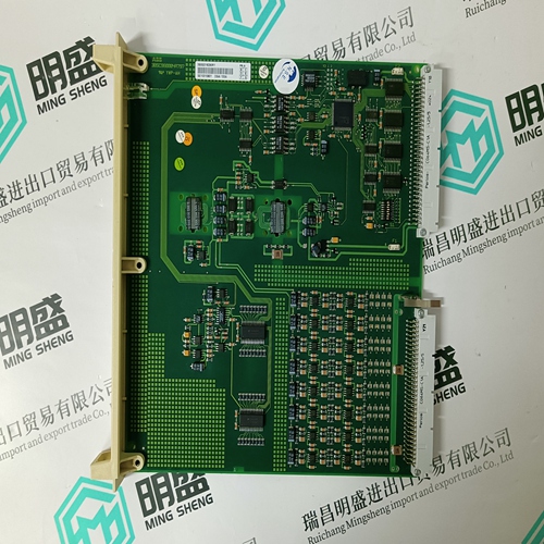
1C31201G01 Analog input module
- Product ID: 1C31201G01
- Brand: EMERSON
- Place of origin: The United States
- Goods status: new/used
- Delivery date: stock
- The quality assurance period: 365 days
- Phone/WhatsApp/WeChat:+86 15270269218
- Email:xiamen2018@foxmail.com
- Tags:1C31201G01Analog input module
- Get the latest price:Click to consult
1C31201G01 Analog input module
As the list is read in from the processor and as the commands are processed, an error value is maintained in the module for each command. This error list can be transferred to the processor. The following tables describe the error codes generated by the module. Note: 125 words is the maximum count allowed by the MODBUS protocol. Some field devices may support less than the full 125 words. Check with your device manufacturer for the maximum count supported by your particular slave.
Normal data transfer includes the paging of the user data found in the module’s internal database in registers 0 to 4999 and the status data. These data are transferred through read (input image) and write (output image) blocks.
Transferring the Command Error List to the Processor
You can transfer the command error list to the processor from the module database. To place the table in the database, set the Command Error Pointer parameter to the database location desired. To transfer this table to the processor, make sure that the Command Error table is in the database area covered by the Read Data.This sequence will continue until interrupted by other write block numbers sent by the controller or by a command request from a node on the MODBUS network or operator control through the module’s Configuration/Debug port.
Read Block and Write Block Transfer Sequences
The Read Block ID is an index value used to determine the location of where the data will be placed in the processor controller tag array of module read data. The number of data words per transfer depends on the configured Block Transfer Size parameter in the configuration file (possible values are 60, 120, or 240). The Write Block ID associated with the block requests data from the processor. Under normal program operation, the module sequentially sends read blocks and requests write blocks. For example, if the application uses three read and two write blocks, the sequence will be as follows: R1W1→R2W2→R3W1→R1W2→R2W1→R3W2→R1W1→

1.Payment method and delivery
Shipment: EMS,DHL,UPS & FEDEX
Payment: T/T or Western Union
2. About us
We are professional company and we are expert in this business, we have highly experienced production team, or sales team, or purchase team, we have most advanced production line. We are reputable in the market.
3. Application industry
Our main products are widely used in metallurgy, oil and gas, glass manufacturing, aluminum, petrochemical, coal mine, paper making and printing, textile printing and dyeing, machinery, electronic manufacturing, automobile manufacturing, tobacco, plastic machinery, electricity, water conservancy, water treatment/environmental protection, municipal engineering, boiler heating, energy, power transmission and distribution, etc.