Home > Product > DCS control system > 3BHE039203R0101 3BHE036204P201 3BHE039204P106 module
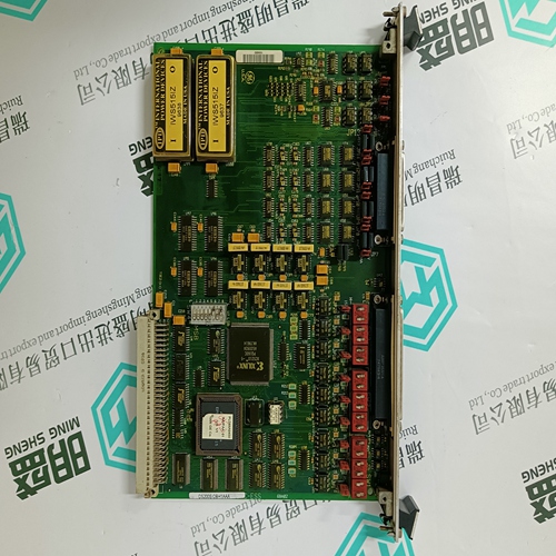
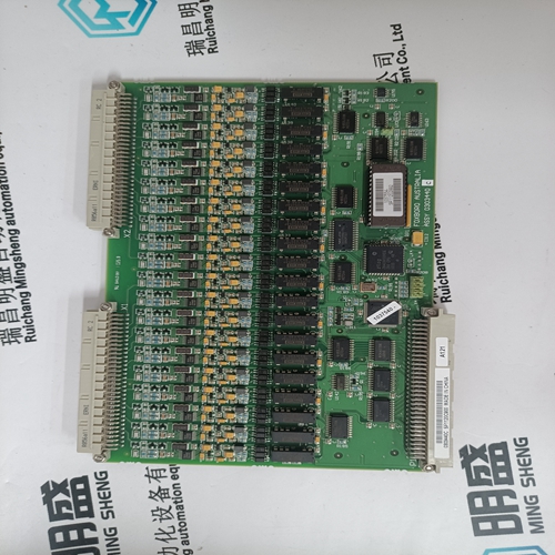
3BHE039203R0101 3BHE036204P201 3BHE039204P106 module
- Product ID: 3BHE039203R0101 3BHE036204P201 3BHE039204P106
- Brand: ABB
- Place of origin: The Swiss
- Goods status: new/used
- Delivery date: stock
- The quality assurance period: 365 days
- Phone/WhatsApp/WeChat:+86 15270269218
- Email:stodcdcs@gmail.com
- Tags:3BHE039203R01013BHE036204P2013BHE039204P106module
- Get the latest price:Click to consult
3BHE039203R0101 3BHE036204P201 3BHE039204P106 module
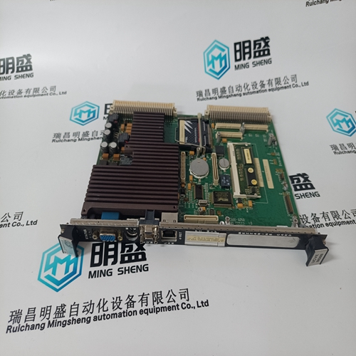
The CPU board contains a shared DRAM area with a capacity of 4, 8, 16 or 32MB. -R-501 CPU-30SEN-R has a default of 32MB DRAM and CPU-30SEN-R-501 has a default of 4MB DRAM. The Shared DRAM area is optimized for fast accesses from the 68030 microprocessor and the DMA controller in the FGA-002 Gate Array. The shared DRAM is also accessible by other APNbus masters. The shared DRAM area is arranged in 36-bit wide memory banks. There may be one or two of these banks on the CPU board, depending on the overall memory capacity delivered. Each 36-bit wide bank is separated into 32 data bits and 4 parity bits. A parity bit checks every eight consecutive data bits (byte parity). Advanced on-board memory control logic routes data to and from the 68030 microprocessor, the DMA controller, and the APNbus interface.
For every read cycle
regardless of size (byte, word, long-word or cache line) and regardless of master (68030, DMA or APNbus), all 32 bits of data and 4 bits of parity are read from the shared DRAM array. The 32 data and 4 parity bits are stored in transceivers. A synchronous termination signal (STERM) is asserted, and the cycle completes. Parity is regenerated in FGA-002 and compared to the parity bits read from memory. If a mismatch is found on an accessed byte, an error will be flagged. The detection of a parity error generates a processor interrupt (programmable inside of the FGA-002)
Write cycles are handled differently.
In the case of a long-word access aligned to a 4-byte boundary, the DRAM can be written immediately. The parity info generated by FGA-002 will be written additionally to the DRAM. A synchronous termination signal (STERM) is asserted, and the cycle completes. For all other write cycles (byte, word, long-word unaligned), the momentary valid parity info stored in DRAM must be read. Then the write to DRAM memory will be performed. Therefore, only the necessary data will be written, the remaining data already stored in DRAM will stay unmodified. Additionally, the new parity info generated by FGA-002 will be merged with the read parity info from DRAM and finally all four parity bits are written to DRAM. The synchronous termination signal (STERM) will be generated to complete the cycle.

Superior products
Main products include DCS control system spare parts, PLC system spare parts and robot system spare parts,
Advantage brands: Allen Bradley, BentlyNevada, ABB, Emerson Ovation, Honeywell DCS, Rockwell ICS Triplex, B&R, FOXBORO, Schneider PLC, GE Fanuc, Motorola, HIMA, TRICONEX, Prosoft and other imported industrial parts
Application industry
Our main products are widely used in metallurgy, oil and gas, glass manufacturing, aluminum, petrochemical, coal mine, paper making and printing, textile printing and dyeing, machinery, electronic manufacturing, automobile manufacturing, tobacco, plastic machinery, electricity, water conservancy, water treatment/environmental protection, municipal engineering, boiler heating, energy, power transmission and distribution, etc.