Home > Product > DCS control system > ABB 3BSE003911R0001 control module
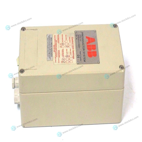
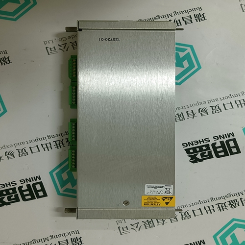
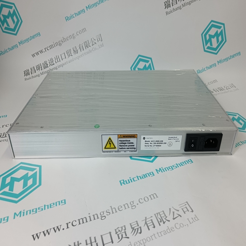
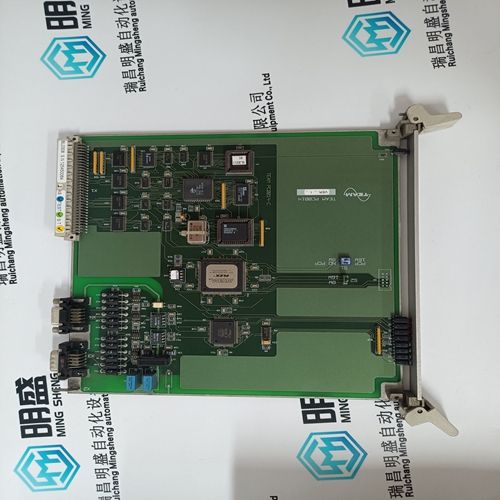
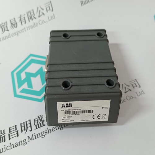
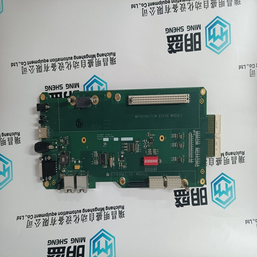
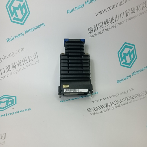
ABB 3BSE003911R0001 control module
- Product ID: 3BSE003911R0001
- Brand: ABB
- Place of origin: The Swiss
- Goods status: new/used
- Delivery date: stock
- The quality assurance period: 365 days
- Phone/WhatsApp/WeChat:+86 15270269218
- Email:xiamen2018@foxmail.com
- Tags:ABB3BSE003911R0001control module
- Get the latest price:Click to consult
ABB 3BSE003911R0001 control module
1 Bank Selection of DRAM The bank selection depends on memory size. The single bank architecture realizes the 4MB and 16MB DRAM variants. The dual-banks architecture realizes 8MB and 32MB DRAM capacity. On CPU-30SEN-R both banks are surface mounted devices. -R-501 On CPU-30SEN-R-501 the second memory bank is realized by a DRAM module.
Shared DRAM byte parity generation and check work for both local and APNbus accesses. If a parity error is detected during a APNbus slave read access, the CPU board drives BERR, informing the APNbus master about the parity error. On all local accesses, a normal STERM will be generated, plus an interrupt on a software programmable level. The access address is stored inside the FGA-002 Gate Array allowing easy software controlled detection of the cycle which caused the parity error.
The Shared DRAM is accessed from the APNbus via FGA-002.
The start and end access addresses are programmable in 4 KByte steps. The defined memory range can be write protected. When the gate array detects a APNbus access cycle to the programmed address range of the Shared DRAM, it requests local bus mastership from the CPU. After the CPU has granted local bus mastership to the FGA-002, the APNbus access cycle is executed and all data is fetched (read cycles), or stored to DRAM (write cycles). The read and write cycle is then terminated and the FGA002 immediately releases local bus mastership. Simultaneously, it completes the fully asynchronous APNbus access cycle. The early completion of the memory read or write cycle allows the CPU to continue processing while the FGA-002 independently manages the APNbus transaction overhead.
A programmable bit within the FGA-002
may be used to disable the early bus release option. With early release disabled, the FGA-002 retains local bus mastership until the APNbus cycle is finished. This guarantees that no other local bus master (CPU or DMA controller) will access the Shared DRAM until the APNbus cycle is complete. In the case of a readmodify-write (RMW) cycle by another APNbus master to the Shared DRAM, the FGA-002 will perform both transactions (a read followed by a write) without releasing the local bus, thus guaranteeing that the cycle is indivisible. In short, the early release option allows the CPU access to the Shared DRAM sooner, but sacrifices the guaranteed indivisibility of APNbus RMW cycles.


Superior products
Main products include DCS control system spare parts, PLC system spare parts and robot system spare parts,
Advantage brands: Allen Bradley, BentlyNevada, ABB, Emerson Ovation, Honeywell DCS, Rockwell ICS Triplex, B&R, FOXBORO, Schneider PLC, GE Fanuc, Motorola, HIMA, TRICONEX, Prosoft and other imported industrial parts
Application industry
Our main products are widely used in metallurgy, oil and gas, glass manufacturing, aluminum, petrochemical, coal mine, paper making and printing, textile printing and dyeing, machinery, electronic manufacturing, automobile manufacturing, tobacco, plastic machinery, electricity, water conservancy, water treatment/environmental protection, municipal engineering, boiler heating, energy, power transmission and distribution, etc.
