Home > Product > DCS control system > TRICONEX 3625C1 Switch module
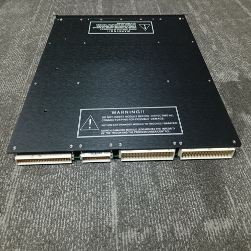
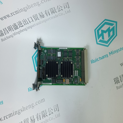
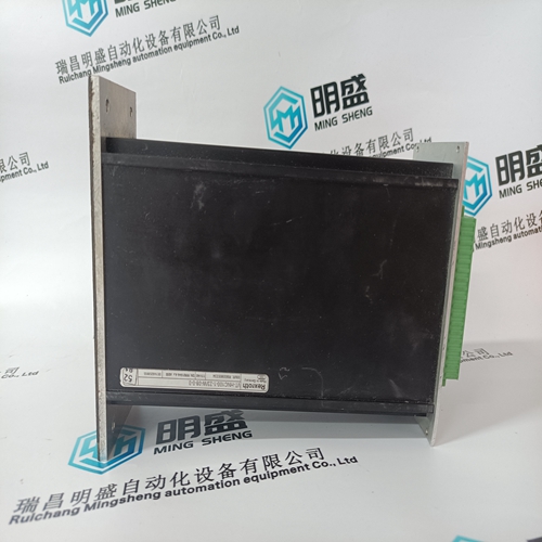
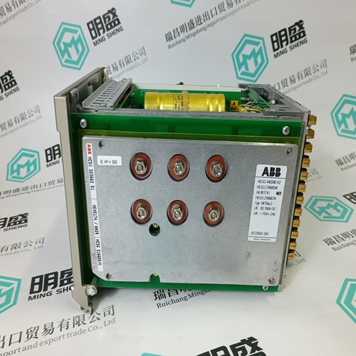
TRICONEX 3625C1 Switch module
- Product ID: 3625C1
- Brand: TRICONEX
- Place of origin: The United States
- Goods status: new/used
- Delivery date: stock
- The quality assurance period: 365 days
- Phone/WhatsApp/WeChat:+86 15270269218
- Email:stodcdcs@gmail.com
- Tags:TRICONEX 3625C1Switch module
- Get the latest price:Click to consult
The main products
Spare parts spare parts, the DCS control system of PLC system and the robot system spare parts,
Brand advantage: Allen Bradley, BentlyNevada, ABB, Emerson Ovation, Honeywell DCS, Rockwell ICS Triplex, FOXBORO, Schneider PLC, GE Fanuc, Motorola, HIMA, TRICONEX, Prosoft etc. Various kinds of imported industrial parts
TRICONEX 3625C1 Switch module
The PQMII contains a user-definable area in the memory map. This area allows remapping of the addresses of all actual values and setpoints registers. The user-definable area has two sections: • A Register Index area (memory map addresses 0180h to 01F7h) that contains 120 actual values or setpoints register addresses. • A Register area (memory map addresses 0100h to 017Fh) that contains the data at the addresses in the Register Index. Register data that is separated in the rest of the memory map may be remapped to adjacent register addresses in the user-definable registers area. This is accomplished by writing to register addresses in the user-definable register index area. This allows for improved throughput of data and can eliminate the need for multiple read command sequences. For example, if the values of Phase A Current (register address 0240h) and Phase A Power Factor (register address 02FDh) are required to be read from a PQMII, their addresses may be remapped as follows: 1. Write 0240h to address 0180h (User-Definable Register Index 0000) using Modbus function code 06h or 10h. 2. Write 02FDh to address 0181h (User-Definable Register Index 0001) using Modbus function code 06h or 10h. A read (function code 03h or 04h) of registers 0100h (User-Definable Register 0000) and 0101h (User-Definable Register 0001) will return the Phase A Current and Phase A Power Factor.
Memory Map Information
The data stored in the PQMII are grouped by setpoints and actual values. Setpoints can be read and written by a master computer; actual values are read-only. All setpoints and actual values are stored as two-byte values; that is, each register address is the address of a two-byte value. In the Modbus memory map, addresses are shown in hexadecimal notation; data values (setpoint ranges, increments, factory values) are in decimal notation.
tion Table The following table lists all objects recognized and returned by the PQMII. Additional information provided on the following pages includes lists of the default variations and defined point numbers returned for each object. Implementation Table Notes: 1. For this object, the quantity specified in the request must be exactly 1 as there is only one instance of this object defined in the relay. 2. All static input data known to the relay is returned in response to a request for Class 0. This includes all objects of type 1 (Binary Input) and type 30 (Analog Input).3. The point tables for Binary Input and Analog Input objects contain a field which defines which event class the corresponding static data has been assigned to. 4. For this object, the qualifier code must specify an index of 7 only. 5. Warm Restart (function code 14) is supported although it is not required by the DNP level 2 specification. 6. Object 1 Variation 1 always indicates On Line for all points