Home > Product > PLC programmable module > Reliance Electric 45C364 Pulse interface card
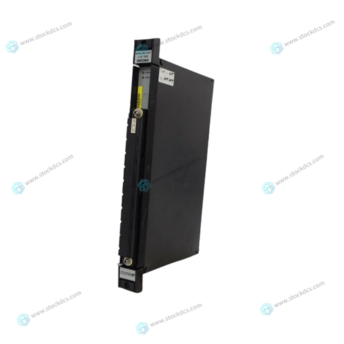
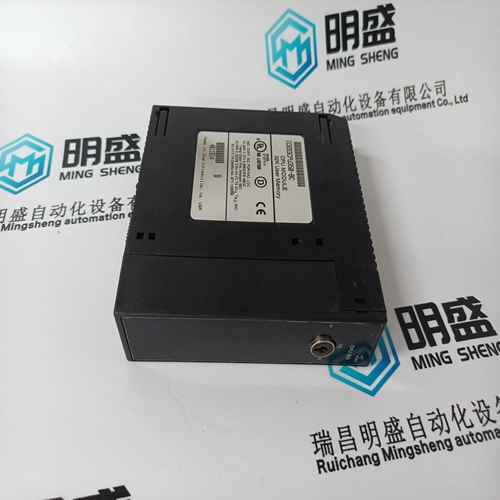
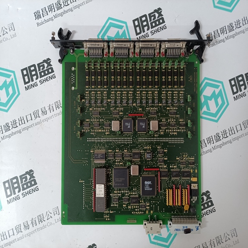
Reliance Electric 45C364 Pulse interface card
- Product ID: 45C364
- Brand: Reliance Electric
- Place of origin: The United States
- Goods status: new/used
- Delivery date: stock
- The quality assurance period: 365 days
- Phone/WhatsApp/WeChat:+86 15270269218
- Email:stodcdcs@gmail.com
- Tags:Reliance Electric45C364Pulse interface card
- Get the latest price:Click to consult
Reliance Electric 45C364 Pulse interface card
For a complete description of the register bits, refer to the data sheet for the specific chip. For a more detailed memory map, refer to the following detailed peripheral device memory maps.
2. The SCC is an 8-bit device located on an MCchip private data bus. Byte access is required.
3. Writes to the LCSR in the VMEchip2 must be 32 bits. LCSR writes of 8 or 16 bits terminate with a TEA signal. Writes to the GCSR may be 8, 16 or 32 bits. Reads to the LCSR and GCSR may be 8, 16 or 32 bits. Byte reads should be used to read the interrupt vector.
4. This area does not return an acknowledge signal. If the local bus timer is enabled, the access times out and is terminated by a TEA signal.
5. Size is approximate.
6. Port commands to the 82596CA must be written as two 16-bit writes: upper word first and lower word second. 7. Refer to the Flash and EPROM Interface section in the MCchip description in Chapter 3
Detailed I/O Memory Maps
Tables 3-3 through 3-12 provide detailed memory maps for the VMEchip2, the MCchip, the Zilog Z85230 serial communications controller, the Intel 82596CA LAN controller, the NCR 53C710 SCSI controller, the IPIC chip, and the MK48T08 BBRAM/TOD Clock.
The MK48T08 BBRAM (also called Non-Volatile RAM or NVRAM) is divided into six areas as shown in Table 3-10. The first five areas are defined by software, while the sixth area, the time-of-day (TOD) clock, is defined by the chip hardware. The first area is reserved for user data. The second area is used by Motorola networking software. The third area is used by the operating system. The fourth area is used by the MVME162 board debugger (MVME162Bug). The fifth area, detailed in Table 3-11, is the configuration area. The sixth area, the TOD clock, detailed in Table 3-12, is defined by the chip hardware.
The fields are defined as follows:
1. Four bytes are reserved for the revision or version of this structure. This revision is stored in ASCII format, with the first two bytes being the major version numbers and the last two bytes being the minor version numbers. For example, if the version of this structure is 1.0, this field contains: 0100 2. Twelve bytes are reserved for the serial number of the board in ASCII format. For example, this field could contain: 000000470476 3. Sixteen bytes are reserved for the board ID in ASCII format. For example, for an MVME162 board with MC68040, SCSI, Ethernet, 4MB DRAM, and 512KB SRAM, this field contains: MVME162-23 (The 10 characters are followed by six blanks.)

Professional seller
Professional sales of major electrical brand products in the world
Overseas direct purchase of products, authentic inventory, price concessions
After sales warranty, complete models, same products, different prices and services