Home > Product > Servo control system > WOODWARD 5500-134 Servo hydraulic
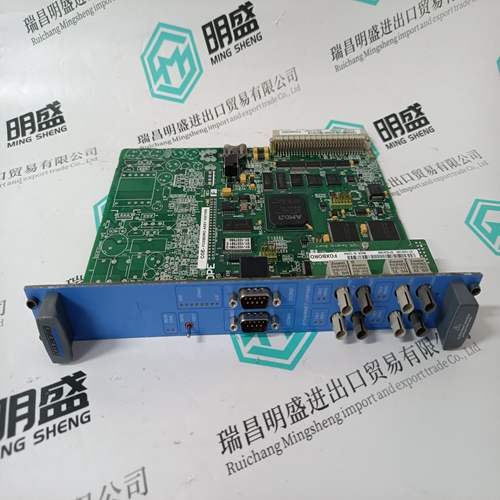
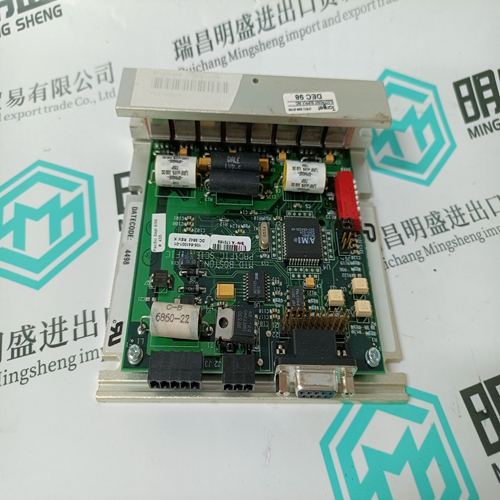
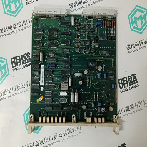
WOODWARD 5500-134 Servo hydraulic
- Product ID: 5500-134
- Brand: WOODWARD
- Place of origin: The United States
- Goods status: new/used
- Delivery date: stock
- The quality assurance period: 365 days
- Phone/WhatsApp/WeChat:+86 15270269218
- Email:xiamen2018@foxmail.com
- Tags:WOODWARD5500-134Servo hydraulic
- Get the latest price:Click to consult
WOODWARD 5500-134 Servo hydraulic
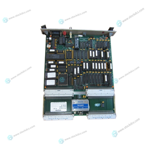
The P bus address map depends on the type of HYPERmodule (mezzanine module) installed and the value written into the PCNFA and PCNFB registers on the main logic board (CPU processor). There are six possible configurations of HYPERmodules: 0, 1, 2, 5, 6, and A. (Each configuration can use MC88200 or MC88204 CMMUs, making a total of 12 possible HYPERmodules.) These configurations are defined in the WHOAMI Register description in Chapter 4. Refer to that section for information on the different HYPERmodule configurations.For example, in an HM88K-1P128-2 configuration 2 HYPERmodule (1 CPU, 8 CMMUs), there are four CMMUs on each P bus (i.e., four on the code side and four on the data side). If PCNFx registers on the main logic board are set to 0, P bus address bits 14 and 12 are decoded to select each CMMU. If the PCNFx are set to 5, however, P bus address bit 14 and the P bus supervisor bit are used to select each CMMU.
M Bus Address Map
The M bus address map is defined in the following sections. Three usable address spaces are available to M bus masters: local DRAM space, VMEbus space, and utility space. In addition, a fourth address space is available which always returns an error. At power-up time (or any time the MADY bit of the CPU ControVStatus Register (CCSR) is = 0), the only access available to M bus masters is utility space. When MADY = 0, utility space is a 4MB block that is repeated throughout the entire 4Gb M bus address space (1024 times). All of the MVME188A registers and the MC88200 and/or MC88204 registers (as well as the VMEbus short 1/0 space) are mapped to addresses within utility space. Refer to Chapter 4 for information on the M Bus Address Decoder and the registers.
DRAM Address Map
The memory board supplied as part of the MVME188A is a 16MB DRAM, 64MB DRAM, or 32MB ECC DRAM board. Note that there are restrictions as to how the DRAM addresses are mapped; some of the M bus address bits are used to select both the 4MB page number and the DRAM address at the same time. Refer to Chapter 4 for information on the M Bus Address Decoder for an explanation of how DRAM address mapping is handled. The decoding is summarized in Table 3-7.


About us
We are professional company and we are expert in this business, we have highly experienced production team, or sales team, or purchase team, we have most advanced production line. We are reputable in the market.
Our products
A company specializes in the sales of module spare parts of global famous brands (DCS system) (robot system) (large servo control system). The company's products include distributed control system (DCS), programmable controller (PLC), MOTOROLA MVME industrial module, industrial control communication converter (Anybus), remote output/input module (RTU), industrial computer (IPC), industrial low screen screen (IPC) HMI SCSI (50, 68, 80Pin) AnyBus (Gateway) has become a global sales enterprise of industrial automation spare parts and components
