Home > Product > Servo control system > HIMA F3113 Integrated circuit card
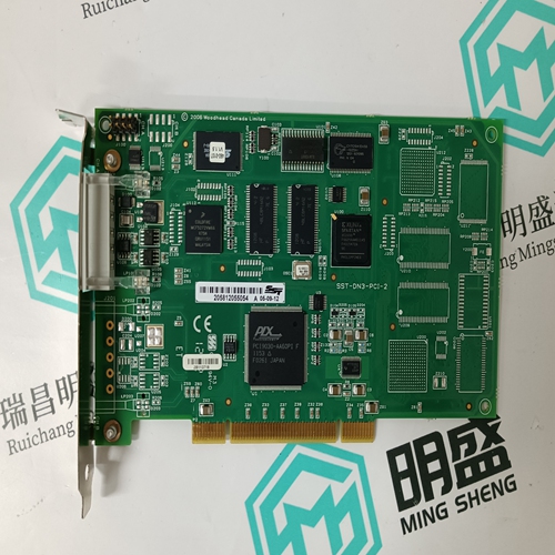
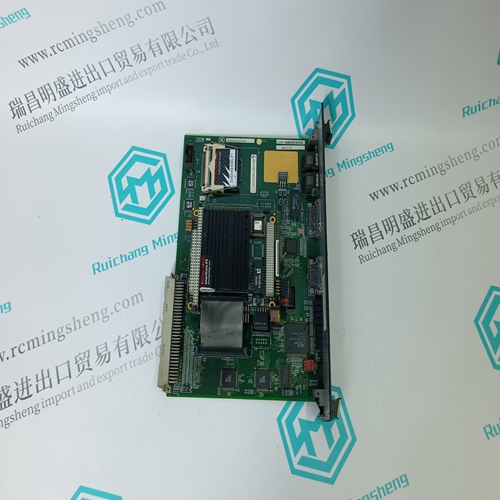
HIMA F3113 Integrated circuit card
- Product ID: F3113
- Brand: HIMA
- Place of origin: Germany
- Goods status: new/used
- Delivery date: stock
- The quality assurance period: 365 days
- Phone/WhatsApp/WeChat:+86 15270269218
- Email:stodcdcs@gmail.com
- Tags:HIMAF3113Integrated circuit card
- Get the latest price:Click to consult
HIMA F3113 Integrated circuit card
At any instant, each RISC processor can generate an access te two of four 4Gb logical address spaces: user code, user data, supervisor code, or supervisor data. Code and data accesses can be simultaneous, because they occur on separate buses. For any access, the selected CMMU immediately resolves the access and, if an M bus access is needed, translates the logical processor address to a physical memory bus access. To obtain a choice of interleaving, an operating system kernel can use the P bus configuration registers on the main logic board. If desired, real time systems can use separate CMMUs for kernel and user tasks so that interrupt response times and critical routine execution times are independent of the cache behavior. Real time systems can also program up to one half of the CMMUs to operate in the SRAM mode and thus guarantee that critical interrupt routines encounter no wait states. The SRAM mode CMMUs can be configured to appear in the kernel logical address space only or in both the kernel and user logical address spaces.
Main Logic Board Registers
The main logic (CPU) board includes eleven registers to facilitate coherent communications with the memory and system controller boards in a VMEbus multiprocessor environment. The following sections describe in detail the main logic board registers and their functions, as well as the state of all bits at powerup time (SRS1) or after an LRST. All registers (with the exception of the GCSR) are located on 4-byte boundaries. Accesses to all of these registers should be 32-bit operations. All accesses to the GCSR should be 8-bit or 16-bit operations. Unless otherwise noted in the register bit descriptions, all undefined bits will be read as "1". Undefined bits are ignored on writes. All of the following registers reside on the main logic (CPU) board.
CPU Control and Status Register (CCSR)
The CCSR,provides the status (on read) and control (on write) of all the hardware functions on the main logic (CPU) board. The bits are all read/write. Bit assignments are shown in Table 4-16. Note that extreme caution should be exercised when changing the state of the MADV or V ADV bits. The V ADV bit is especially dangerous to modify, because the other VMEbus masters are not necessarily under direct control of the MVME188A. Any VMEbus A24 or A32 slave accesses (by these other masters) to MVME188A resources are ignored when V ADV is clear. This may cause system problems if other VMEbus masters depend on MVME188A resources to function properly. This register is cleared by SRST or LRST.

About us
We are professional company and we are expert in this business, we have highly experienced production team, or sales team, or purchase team, we have most advanced production line. We are reputable in the market.
Our products
A company specializes in the sales of module spare parts of global famous brands (DCS system) (robot system) (large servo control system). The company's products include distributed control system (DCS), programmable controller (PLC), MOTOROLA MVME industrial module, industrial control communication converter (Anybus), remote output/input module (RTU), industrial computer (IPC), industrial low screen screen (IPC) HMI SCSI (50, 68, 80Pin) AnyBus (Gateway) has become a global sales enterprise of industrial automation spare parts and components