Home > Product > DCS control system > ABB SDCS-PIN-46-COAT 3BSE004939R1003 Logic conversion module
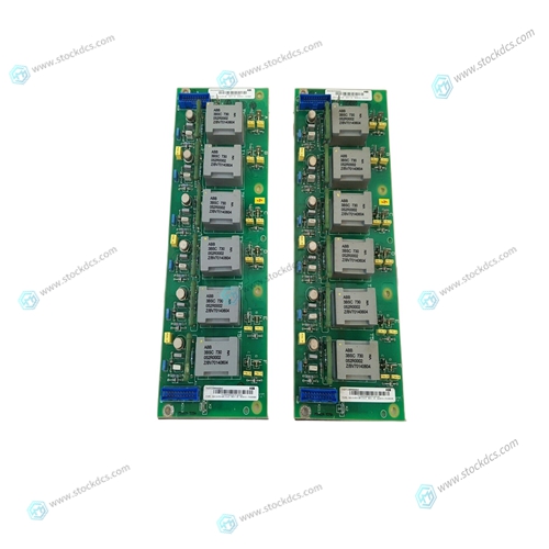
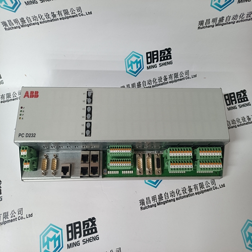
ABB SDCS-PIN-46-COAT 3BSE004939R1003 Logic conversion module
- Product ID: SDCS-PIN-46-COAT 3BSE004939R1003
- Brand: ABB
- Place of origin: The Swiss
- Goods status: new/used
- Delivery date: stock
- The quality assurance period: 365 days
- Phone/WhatsApp/WeChat:+86 15270269218
- Email:stodcdcs@gmail.com
- Tags:ABBSDCS-PIN-46-COAT3BSE004939R1003Logic conversion module
- Get the latest price:Click to consult
ABB SDCS-PIN-46-COAT 3BSE004939R1003 Logic conversion module
Two SQUELCH modes are available with the ADN2816. SQUELCH DATAOUT and CLKOUT mode is selected when CTRLC[1] = 0 (default mode). In this mode, when the SQUELCH input, Pin 27, is driven to a TTL high state, both the clock and data outputs are set to the zero state to suppress downstream processing. If the SQUELCH function is not required, Pin 27 should be tied to VEE. SQUELCH DATAOUT or CLKOUT mode is selected when CTRLC[1] is 1. In this mode, when the SQUELCH input is driven to a high state, the DATAOUTN/DATAOUTP pins are squelched. When the SQUELCH input is driven to a low state, the CLKOUT pins are squelched. This is especially useful in repeater applications, where the recovered clock may not be needed.
I 2 C INTERFACE
The ADN2816 supports a 2-wire, I2 C compatible, serial bus driving multiple peripherals. Two inputs, serial data (SDA) and serial clock (SCK), carry information between any devices connected to the bus. Each slave device is recognized by a unique address. The ADN2816 has two possible 7-bit slave addresses for both read and write operations. The MSB of the 7-bit slave address is factory programmed to 1. B5 of the slave address is set by Pin 19, SADDR5. Slave Address Bits [4:0] are defaulted to all 0s. The slave address consists of the 7 MSBs of an 8-bit word. The LSB of the word either sets a read or write operation (see Figure 6). Logic 1 corresponds to a read operation, while Logic 0 corresponds to a write operation.
To control the device on the bus
the following protocol must be followed. First, the master initiates a data transfer by establishing a start condition, defined by a high-to-low transition on SDA while SCK remains high. This indicates that an address/ data stream follows. All peripherals respond to the start condition and shift the next eight bits (the 7-bit address and the R/W bit). The bits are transferred from MSB to LSB. The peripheral that recognizes the transmitted address responds by pulling the data line low during the ninth clock pulse. This is known as an acknowledge bit. All other devices withdraw from the bus at this point and maintain an idle condition. The idle condition is where the device monitors the SDA and SCK lines waiting for the start condition and correct transmitted address. The R/W bit determines the direction of the data. Logic 0 on the LSB of the first byte means that the master writes information to the peripheral. Logic 1 on the LSB of the first byte means that the master reads information from the peripheral.


Company introduction
Temporal Ming sheng automation equipment co., LTD. Was established in April 02, 2021, registered jiujiang ruichang city in jiangxi province, east yi road no. 23 lake farmers 401 mall, the legal representative person Zhou Zuochen.
[Main Products]
Main products: PLC and DCS system spare parts modules of world famous brands
①Allen-Bradley 1756、1746、1747、1771、1785
②Schneider 140 Series PLC module
③General electric GE
IC693 IC697 IC698 Series PLC module
DS200 DS3800 DS215 IS200 IS215 IS220 Series gas turbine module
VMIVME Control module of series
④Bently:3500 series cards 3500/22M、3500/15、3500/92 And other products
⑤ICS TRIPLEX
⑥ABB Robots. FANUC Robots、YASKAWA Robots、KUKA Robots、Mitsubishi Robots、OTC Robots、Panasonic Robots、MOTOMAN Robots。
⑦EMERSON:Spare parts for OVATION system, WDPF system and MAX1000 system.
⑧ Invensys Foxboro: I/A Series system, FBM (field input/output module) sequential control, ladder logic control, accident recall processing, digital analog conversion, input/output signal processing, data communication and processing, etc. Invensys Triconex: redundant fault-tolerant control system, Zui modern fault-tolerant controller based on triple module redundancy (TMR) structure.
⑨Woodward:505 series governor 9907-164 And other products
⑩Bosch Rexroth:Indramat,I/O module,PLC CPU,Motors, drives and other products.
◆Motorola:MVME 162、MVME 167、MVME1772、MVME177and other products.
